
Diagnostic Methods
The following diagnostic methods are available to members and other institutions at the Plasma Science Hub:
- Fourier-Transform Infrared Spectroscopy (FTIR)
- X-ray Photoelectron Spectroscopy (XPS)
- Mocon
- Scanning Electron Microscope (SEM)
- Defect diagnostics
- Multi Resonance Probe (MRP)/Plasma Absorption Probe (PAP)
- Energy Resolved Mass Spectrometry
- Phase Resolved Optical Emission Spectrscopy (PROES)
Defect diagnostics
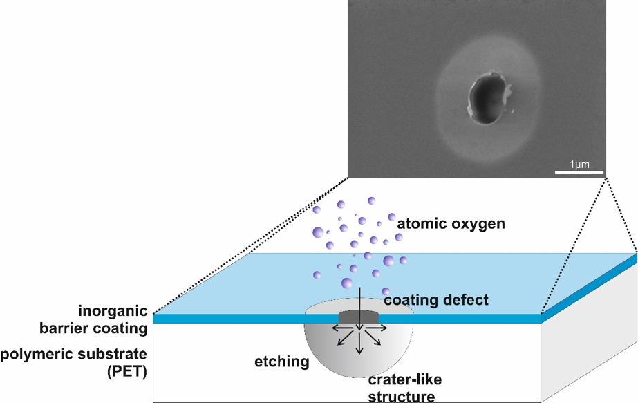 In the field of encapsulation of microelectronics or packaging industry the application of plastics is wide spread, due to their cost efficiency and easy processing. Especially, in packaging industry polyethylene terephthalate (PET) and polypropylene are the dominating material. Nevertheless, plastics offer only limited barrier performance against permeation of gases, e.g. oxygen or CO2. A significant increase of barrier performance can be achieved by the deposition of thin inorganic films by means plasma processes. However, these kind of plasma coatings contain microscopic defects which limit the resulting barrier performance. Usually, these kind of defects are not visible with optical or electron microscopy. Hence, visualization of defects is applied by reactive oxygen etching. This is based on etching the polymer surface underneath coating defects by reactive oxygen species and subsequent imaging with SEM. Most organic polymers like PET are sensitive towards etching by reactive oxygen species. In contrast to this, most inorganic materials like SiOx and TiO2 are almost chemically inert with respect to reactive oxygen species and therefore, etch rates are typically below detection limit. Hence, the inorganic barrier coating serves as a mask against etching and protects the polymer beneath. Nevertheless, reactive oxygen species like atomic oxygen can enter defects and etch the unmasked polymer surface at defect sites. Due to scattering of atomic oxygen in the gas phase etching occurs nearly isotropic, resulting in undercutting of the barrier coating. Subsequently, a crater-like structure is formed. In SEM images, this structure appears as a dark spot in the center surrounded by a whitish circular ring. The dark spot represents the defect, i.e. hole in the barrier film. The number of defects and associated defect density are then determined by an automatized image recognition software, based on the image processing toolbox in MATLAB.
SEM
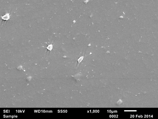 The JEOL JSM-6510 is a Scanning Electron Microscope (SEM). It achieves visualization of a sample by irradiating a focused beam of electrons producing secondary electrons at the surface. Collecting the secondary electrons by means of a detector results in an image of the topography. This enables scanning of a sample with a magnification of up to x300.000 with a resolution of 3 nm using a 30 kV electron beam. The accelerating voltage can be varied between 0.5 and 30 kV.
Mocon
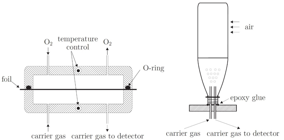 The MOCON OX-TRAN Model 2/61 is an oxygen permeation measurement system. Oxygen transmission through plastic foils or packages is analyzed in six independent cells by means of the carrier gas method. Each cell is sealed and consists of two parts which are separated by a plastic sample. One part is flushed with 100 % oxygen or ambient air. The other part is flushed with forming gas which serves as carrier gas. Oxygen which had permeated through the plastic, is transported to an electrochemical sensor responsible for the measurement. Oxygen Transmission Rate (OTR) can be obtained as a function of temperature in a range from 20°C to 65°C and as a function of relative humidity (RH) between 35 % to 100 %. Measurements are performed for plastic foils with a sample area of 10 cm² or plastic packages (like PET bottles).
PROES
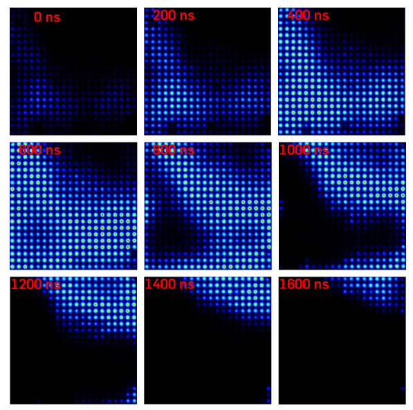 Phase resolved optical emission spectroscopy (PROES) is a technique that alows the investigation of the discharge emission according to the time, especially, phase of the applied excitation voltage. In addition, the combination of an ICCD-Chip and optical filter establishes the spatial resolution of the emission of a selected in wavelenghts.
Here, the camera (LaVison PicoStar HR16) works with a time resolution of about 100 ps. The ICCD-Chip has 512x512 pixels and enables a spatial resolution of few µm. The camera can detect emission in range between 350 nm and 750 nm.