
Plasmas facilitate the production of small structures
Martin Hoffmann explains why plasma processes are essential for microsystem technology and which opportunities they offer for eco-friendly manufacturing methods.
Plasmas are the tool of choice for microsystem technology. As electronic chips are getting smaller and smaller, structures can only be realized with dry, plasma-assisted processes. Wet chemical processes no longer work in these dimensions. During drying, small, movable structures are glued together by surface tension, just as two sheets of glass with a very thin film of water between them can hardly be separated. New materials such as glasses or 2D semiconductors require new processes for deposition and structuring.
The key is specially adapted plasmas. In addition, we need to significantly advance the methods for measuring the internal parameters of a plasma and the relevant process control in real time. This is the only way we can also achieve reproducible results in batch production. In addition, plasma processes offer resource-saving, environmentally friendly manufacturing methods with minimal material input – even when coating with new types of materials. This future begins now, with the construction of research facilities at the boundary between basic and applied research and cross-disciplinary cooperation to enable the use of innovative materials.
Lukas Mai receives a PhD award
 Dr. Lukas Mai from the Faculty of Chemistry and Biochemistry receives a prize from the German Chemical Society (GDCh). The prize is the H.C. Starck Tungsten Doctoral Award 2021 of the GDCh Division of Solid State Chemistry & Materials Research. The prize is awarded for Mai's dissertation "Investigation of Amino-Alkyl Coordinated Complexes as New Precursor Class for Atomic Layer Deposition of Aluminum, Tin and Zinc Oxide Thin Films and Their Application." The certificate and the prize money of 2,500 euros will be awarded at the Science Forum Chemistry at the end of August.
The award-winning work was carried out in an interdisciplinary environment between chemistry, materials science and engineering in the Chemistry of Inorganic Materials group. It involved the investigation of new chemicals, known as precursors, used for the deposition of ultrathin films by atomic layer deposition. These nanostructured thin films could then be tested in current applications as gas sensors, gas barrier layers or in transistors. The two projects SFB-TR 87 and EFRE-FunALD, within which the work was carried out, provided the ideal platform for this application-oriented research.
Atomic Layer Deposition is used in microelectronics for computer chips, displays and sensors, among other applications, to deposit various materials with a thickness of a few nanometers (one millionth of a millimeter) on surfaces. Chemical compounds, known as precursors, are used for this purpose, which must be volatile, thermally stable and reactive. Alkyl compounds are often used in industry, but although they meet these conditions, they self-ignite in air and thus require high safety precautions. Lukas Mai used a so-called 3-(dimethylamino)propyl (DMP) ligand to stabilize aluminum, tin and zinc compounds, which are thus safer and still meet all precursor conditions.
adapted from RUB, Arne Dessaul
Plasma generators control catalytic processes
In ten years, researchers will have understood the interactions between catalysts, which determine the speed of chemical reactions, and plasmas. This will facilitate the excitation of the plasma at atmospheric pressure in such a way that its properties accelerate the reactions on the catalyst surface in a controlled manner. As a result, chemical engineers will not only increase the turnover of the starting materials, but also the percentage of these materials that will be converted into the required product.
Therefore, the vision is that plasma generators will control catalytic processes. New compact plasma catalyst modules will be created, through which large gas flows can pass with little pressure drop. This will enable exhaust gas streams to be purified and other important industrial reactions to be carried out. In order for the modules to work in a resource-saving way, researchers still have to boost their energy efficiency. In future, catalysis, plasma and reaction engineering experts will work hand in hand to develop plasma catalyst modules. Computer-aided plasma, velocity and flow simulations will help to optimise them.
by Martin Muhler
How cola still tingles after a year
When you add energy to gases or gas mixtures, a plasma can be created, and inside it things go haywire: atoms turn into ions, free electrons whiz through space and collide with everything, some ingredients decay, other substances form anew. Depending on what is added to the starting material, plasmas can therefore be used to produce larger compounds. Hydrocarbons and silicon hydrogens are turned into long chains of molecules called polymers.
“If you want to etch with plasmas that tend to form polymers, it’s bad because the nanoparticles that form are a hindrance,” explains Professor Peter Awakowicz, holder of the Chair of General Electrical Engineering and Plasma Technology at RUB. But his team has taken advantage of the situation. If polymers are specifically made to form and deposit on the surfaces surrounding the plasma, they can be coated in a targeted manner. Thanks to this so-called Plasma Enhanced Chemical Vapor Deposition, or PECVD for short, it is possible, for example, to apply ultra-thin, gas-tight coatings to the inside of PET bottles, ensuring that the contents last longer, or to protect organic light-emitting diodes (OLEDs) from moisture so that the TV screens work for a long time. This and much more is only possible because the plasmas are cold and thus do not damage the PET bottle or other surfaces to be coated with heat. Only the fast electrons in the plasma are hot, and they do not damage the surfaces.
Making milk and medicines last longer
The glass-like coating of the plastic, which is only 20 to 30 nanometres thin, ensures that 10 to 100 times less gas escapes through the bottle. This extends the shelf life of a soda pop from the previous four weeks to about a year. The method is also of interest for the packaging of milk and other foods, as well as medicines and even microelectronic components.
“This type of coating is also environmentally friendly, because the tiny amount of material can simply be neglected during recycling,” explains Dr. Marc Böke from the Experimental Physics II department at RUB. Composite materials made of plastic and aluminum, such as Tetrapaks, are far more difficult to recycle because it is very difficult to separate the components.
Other applications of the PECVD method can be, for example, the coating of implants that grow into the bone better than conventional ones. There are also many microelectronic applications. For example, transistors can be deposited with ultrathin silicon dioxide films in plasma.
Oxygen tips the scales
The challenge lies in controlling the formation of the layers. “The layers should not only be ultra-thin, but also absolutely dense, gap-free and uniform,” explains Marc Böke. The adjusting screws for this are manifold. For one thing, it depends on the gas mixture. Atomic Oxygen is a particularly important player. Its proportion can be used to control, among other things, whether other additives evaporated into the plasma form inorganic layers, such as the glass-like silicon dioxide, or organic layers that have other interesting properties, such as giving surfaces greater biocompatibility or enabling gas separation.
The pressure at which the plasma is operated is also significant. Higher pressures and corresponding gases result in the coating of surfaces, while lower pressures are more likely to result in etching processes, which are central to all microelectronics (from cell phones to modern cars). Similarly, the geometry of the reactor and the choice of energy source influence what happens in the plasma and how it affects the surrounding surfaces. For example, an appropriate plasma can be ignited by microwaves, but also by inductively or capacitively coupled radio frequency. “In general, different sizes of plasma reactor are possible, up to the huge dimensions needed to coat entire window panes for high-rise buildings,” says Peter Awakowicz. These coatings serve to reflect infrared radiation that would otherwise cause it to get as hot behind them as in a greenhouse when the sun shines. But you can still see through it. With the sputtering of thin metal layers on foils used for this purpose, it is also possible to work in a feed-through process and thus coat many square metres.
Measurement techniques had to be developed
Only after the basic mechanisms of high-power pulsed sputtering (HiPIMS) and PECVD had been measured and understood in the first phase of the Collaborative Research Center SFB/TR 87 the research teams could get down to the business of implementing such large-area coatings. “We had to develop the appropriate measurement techniques in some cases,” Awakowicz recounts. “If you simply hold a measuring probe in the plasma, it may become coated itself and may lose its function,” he gives an example.
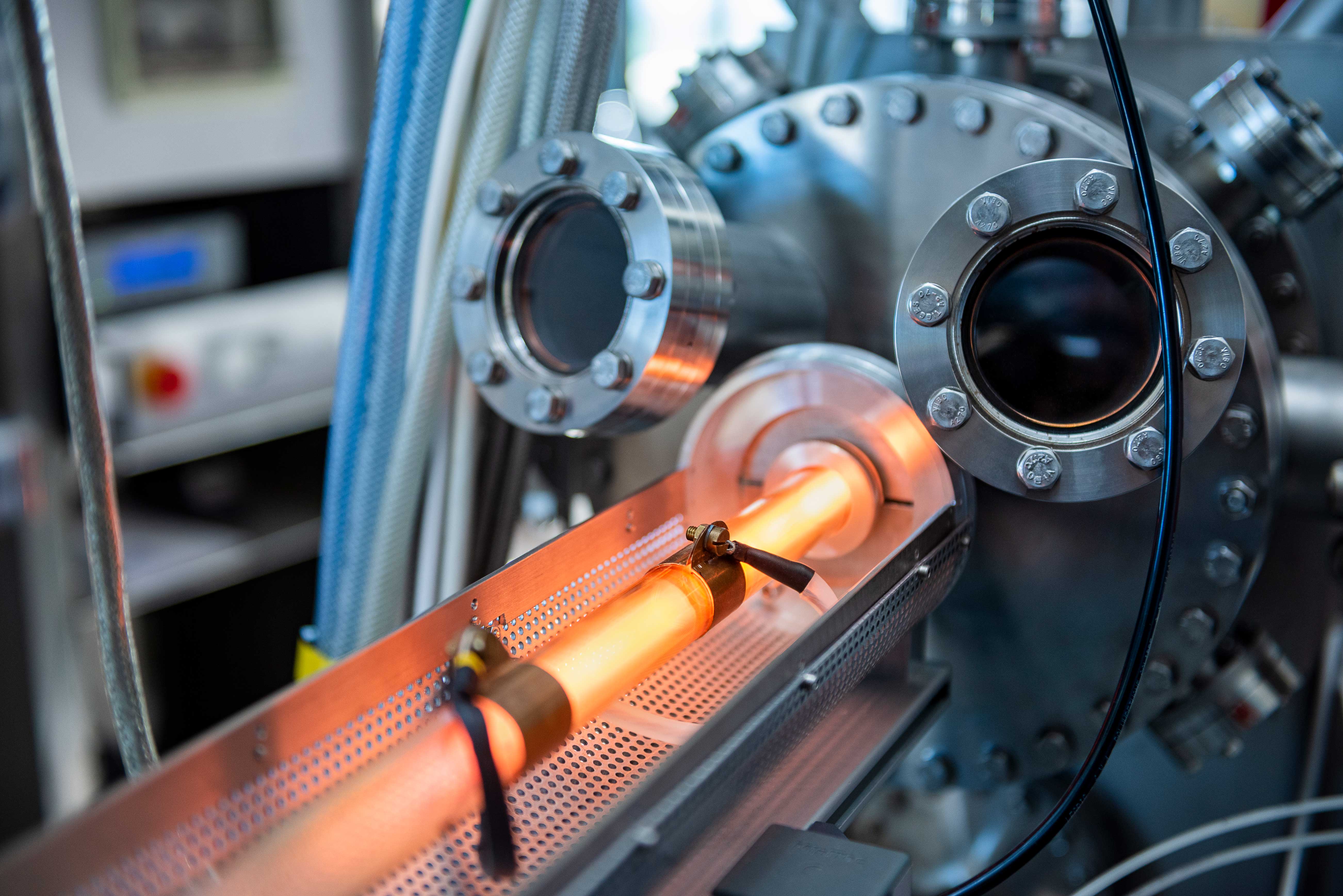
The researchers have gradually been able to fathom and perfect many aspects of the possible processes. For example, PET bottles are cleaned and activated before coating, also by means of plasma. But here, too, the surface of the bottle changes, which in turn influences the subsequent coating. Measurements of the particle flows during cleaning revealed what happens in the process: is wettability increased? And if so, how? Does the surface energy change? At what point in the treatment does the surface become roughened? “If the surface is too rough, you can no longer cover it evenly with an ultra-thin coating,” explains Marc Böke. If all these aspects are taken into account during cleaning and the process is run optimally, this has a considerable influence on the success of the subsequent coating: “We were able to increase the impermeability, which was initially a factor of 100 (depending on the substrate material), to a factor of 500 through the correct setting of the previous cleaning,” says Peter Awakowicz.
Keeping plasticizers away from food
Detailed knowledge of the processes in the plasma and the resulting coatings now also make it possible to coat stretchable films with gas-tight thin films. Thanks to an intervening buffer layer, Marc Böke’s team was able to increase the tolerance of the layer to the stretching of the film from originally about three to about six percent. This application is also of interest to the food industry, for example, as the dense coating prevents ingredients from the film, such as the dreaded plasticizers, from penetrating the food.
The latest application, which is currently being worked on, makes a virtue out of necessity: if one actually wishes for layers that are as dense and defect-free as possible, defects such as tiny pores in the coating are almost impossible to avoid. They allow the research teams to use plasma coating to develop non-swelling filter membranes that exhibit previously unknown properties. They can desalinate water or separate gases from each other, such as oxygen from CO2. “Normally, the more selective a membrane is, the lower its transmission, i.e. the more inefficient the process,” explains Marc Böke. “With plasma coating, however, we can control pore formation so that selectivity no longer comes at the expense of transmission or efficiency.” The researchers of the SFB/TR87 can simulate and tailor the polar properties of the membrane. This makes it easier for certain molecules to pass through the membrane. “Water molecules, for example, are made to give up their actual angle, practically flattening out and thus sliding through the pore,” Peter Awakowicz describes. “You couldn’t target something like that before.”
adapted from Meike Drießen (RUB)